Contact : 301-831-0063
/
e-mail : office@choicecomm.com


Public Sector Product Solutions
Water Treatment, Information Technology, and HVAC Products
For Federal, State, and Local Government
IT Products
IT Infrastructure products for Communications Networking, power, HVAC, Secure KVM, remote & local KVM for Server Access, Racks, Cabling, and more.
HVAC Products
Thermal management solutions promise the world’s most reliable, sustainable, and cost effective heat management for critical spaces.
Water Treatment Products
Engineered with advanced media, our solutions remove impurities, inhibit scale formation and provide a constant flow of water to your equipment.
Pre & Post Sales Support
Support is everything. Our most important customer support comes after the sale. We are in it for the long term with you!
TAA Compliant Products
We sell only sell products that are made in the USA or a Trade Agreements Act (TAA) Country.
Kinetico Water Treatment Differentiators
Lowest pressure drop, highest flow rates available. Longest filter life and lowest cost per 1,000 gal.
We Are Specialists For
Helping You Lighten Your Workload!

How Choicecomm Started
Founded in 2003 by Woody Story, Choicecomm started by becoming a product reseller of IT Networking Products to Federal, State, and Local government customers.

Product Selection & Applications Support
Choicecomm prides itself in providing pre and post sales technical support for selecting and subsequently using the products effectively. We are always here!

Staying Available For You
We endeavor to always be available for Technical, Accounting, and GSA related questions, resources, quotations, and other important needed information.

Why Purchase Products From Us?
It seems like a simple thing……just order some products…right? This would be true until you quickly need to find the best price, delivery, and support. It takes a long time to learn which manufacturers or suppliers are effective, what the price incentives are, establish working relationships, establish financing, and all the processes that get the right product to do the right job on-time. This is what many customers don’t have the time to chase down, so they can rely on Choicecomm to do it for them.
It seems like a simple thing……just order some products…right?

We Help Our Clients to Achieve Their Goal
Resources

KineticoPRO Water Systems
Why Is Your Water Causing Stains?
What causes hard water stains, iron stains and low pH stains, and how can you prevent them?
What is Hard Water?
According to the US Geological Survey, 85% of water in the United States is hard. Learn about hard water today!
Bottled Water vs. Filtered Water
Learn about the differences between in-home water filtration and bottled water.

HVAC
Thermal Management
High-performance thermal management solutions from Vertiv promise the world’s most reliable, sustainable, and cost effective heat management for critical spaces.
IT Solutions
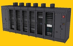
Racks & Enclosures
Vertiv data center racks, cabinets, and enclosure solutions provide modular support and protection to critical IT and facilities.